Test fixture design · Electronics consulting 测试治具设计 · 电子工程顾问

We design the test fixtures that bring advanced electronics to life. 我们设计让先进电子产品精准验证的测试治具。

Corgent is an independent electronic-design and test-engineering consultancy. We design ICT/FCT fixtures, probe cards, load boards and the hardware around them — turning complex test requirements into validated, build-ready designs. 科進是一家独立的电子设计与测试工程顾问公司。我们设计 ICT/FCT 测试治具、探针卡、负载板及相关硬件,将复杂的测试需求转化为经验证、可制造的设计方案。

Independent
Vendor-neutral engineering厂商中立的工程视角
Multi-disciplinary
Mechanical · electrical · software机械 · 电气 · 软件一体
Hong Kong
Design & engineering base设计与工程基地
FCT FIXTURE · DESIGN
Precision test probes contacting a circuit board on a Corgent test fixture
TEST POINTS
4096
NETS
1,280
LAYERS
12
DFTDesign-for-test可测试性设计
Probe CardWafer-level test晶圆级测试
We design for high-reliability industries服务于高可靠性行业
SEMICONDUCTORAUTOMOTIVE · EV5G & TELECOMMEDICALCONSUMERAEROSPACEINDUSTRIAL IoT SEMICONDUCTORAUTOMOTIVE · EV5G & TELECOMMEDICALCONSUMERAEROSPACEINDUSTRIAL IoT

Design-for-test from day one从设计之初就考虑测试

Testability is engineered into the design — not bolted on at the end.将可测试性融入设计之初,而非在末端补救。

One multi-disciplinary team多学科一体团队

Mechanical, electrical and software engineering working together.机械、电气与软件工程协同作战。

Independent & vendor-neutral独立 · 厂商中立

We recommend what's right for your product — not a product line we sell.我们只推荐最适合您产品的方案,而非自家产品。

Confidential by default默认保密

NDA-first engagements and careful handling of your IP.以保密协议为前提,谨慎对待您的知识产权。

What we do核心能力

A design partner for test & electronics测试与电子设计的工程伙伴

From bed-of-nails fixtures to wafer-level probe cards and the boards they validate — Corgent brings mechanical, electrical and software design together as one engineering team.从针床治具到晶圆级探针卡,再到被验证的电路设计,科進以一体化工程团队整合机械、电气与软件设计。

01

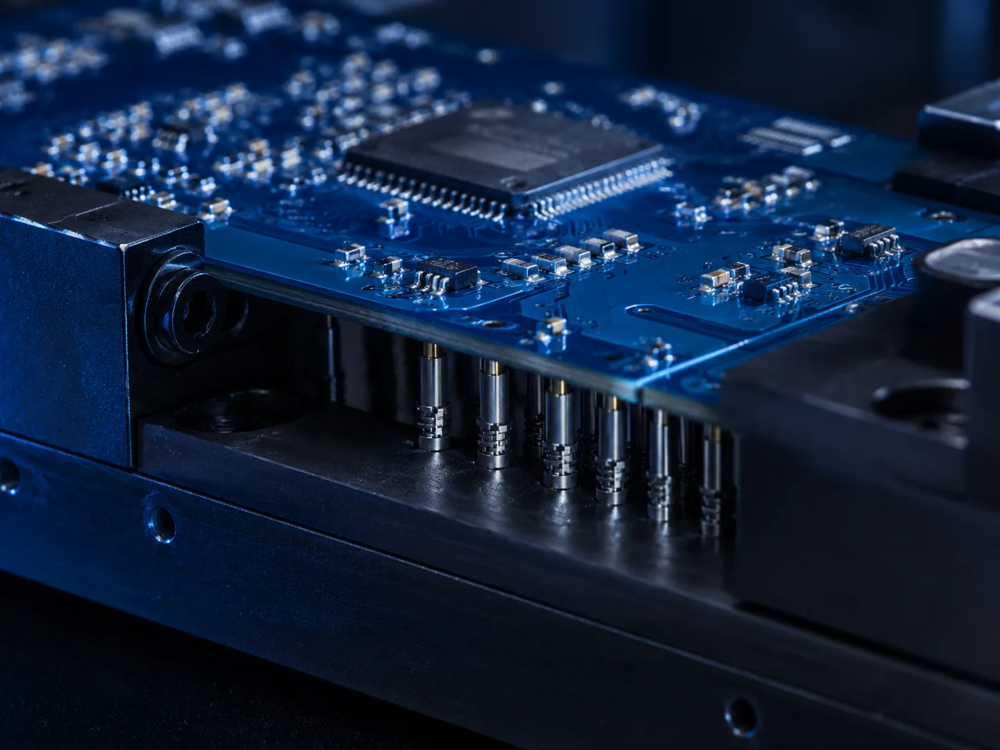
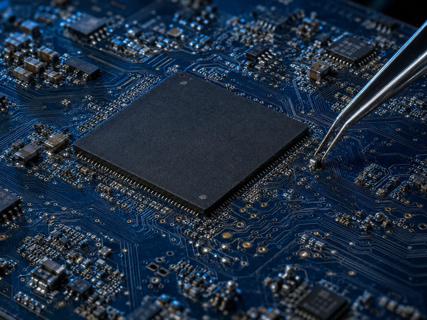
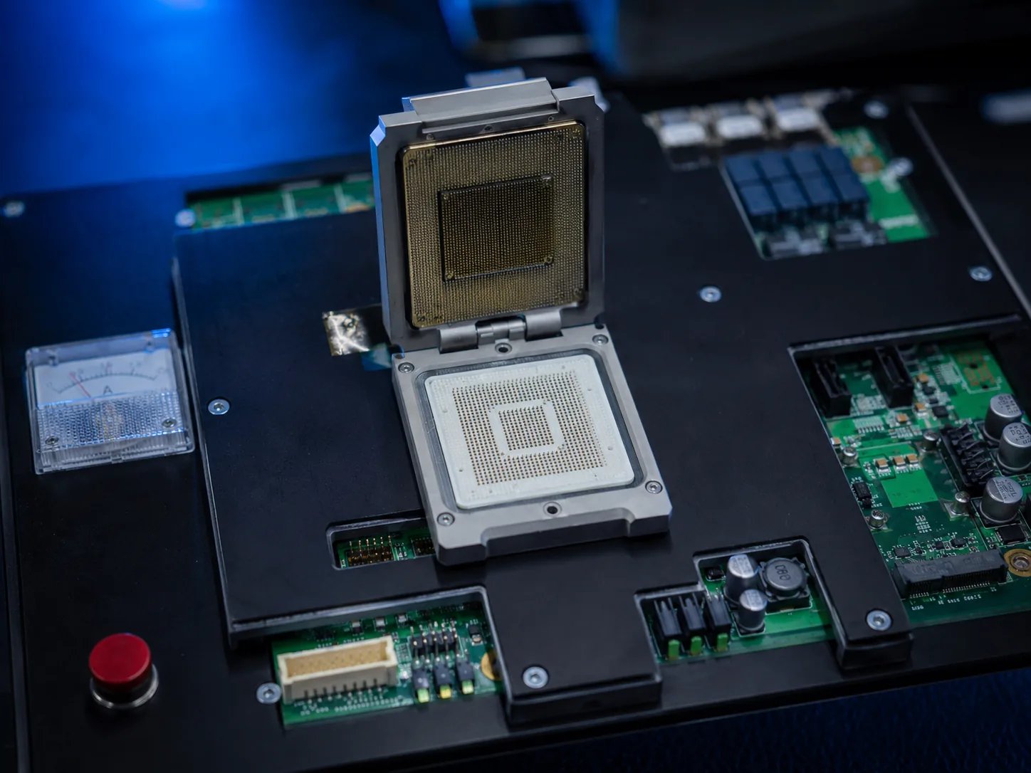
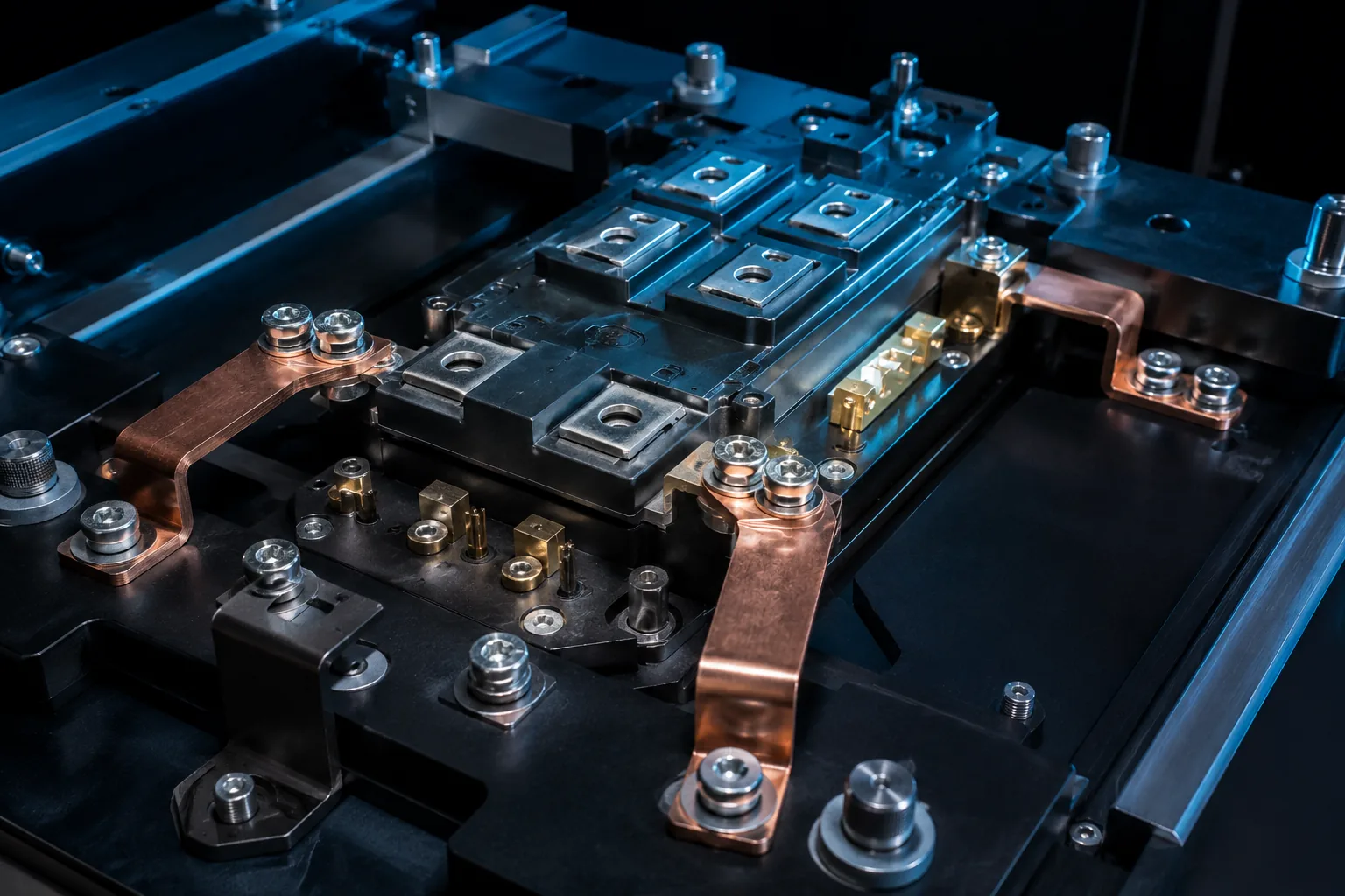
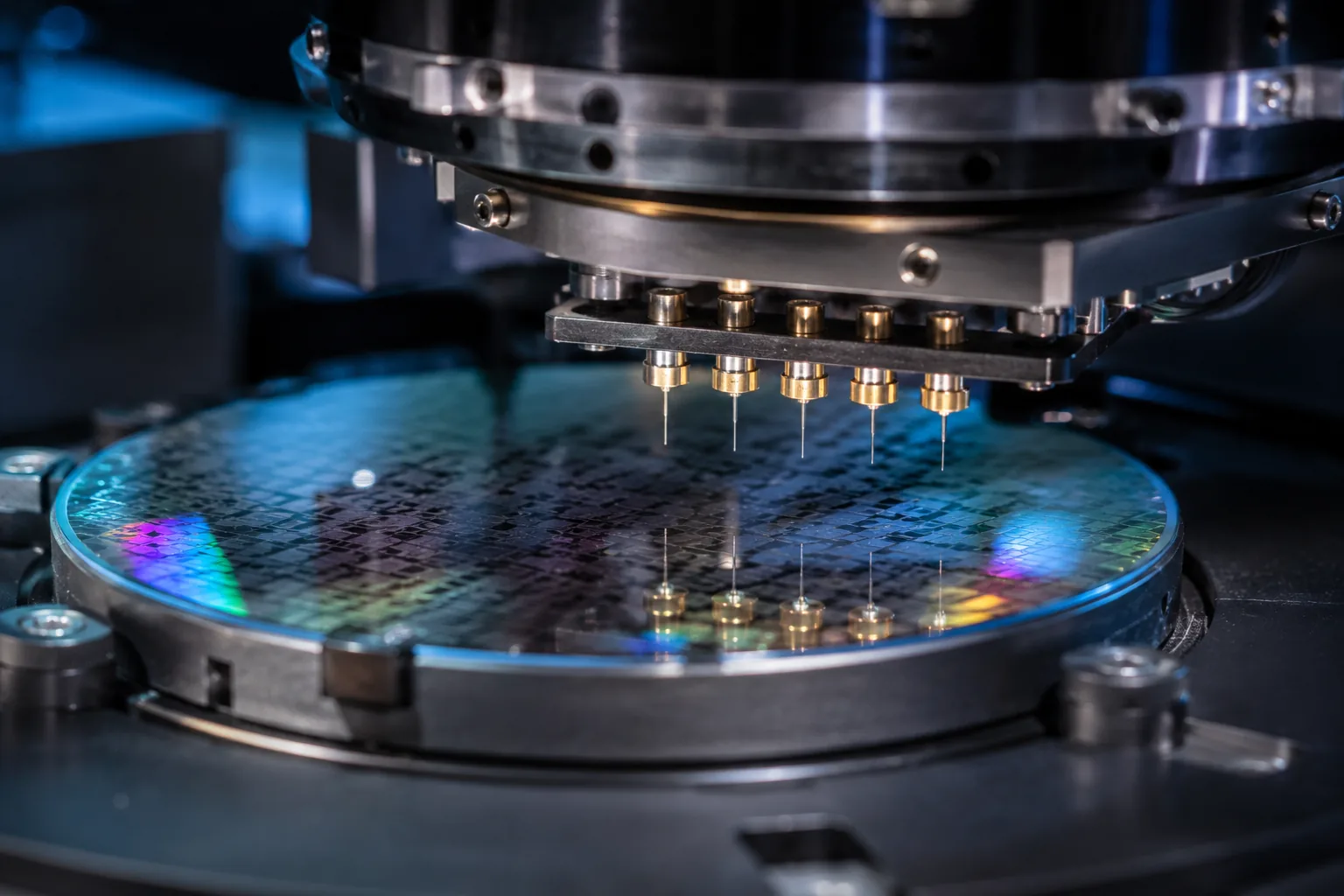
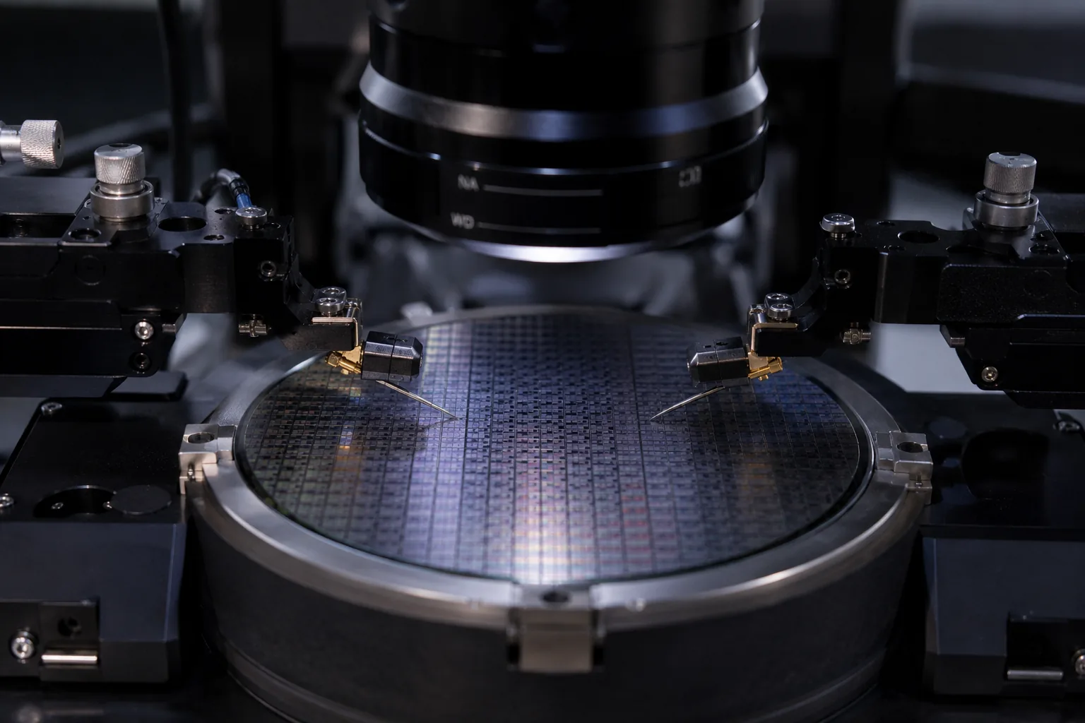
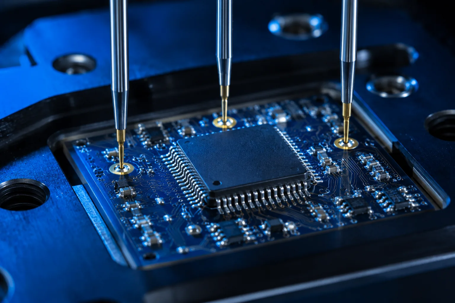
ICT / FCT Fixture DesignICT / FCT 治具设计

We design bed-of-nails, flying-probe and functional test fixtures for repeatable contact, fast changeover and rugged production-line life.设计针床、飞针与功能测试治具,确保接触可靠、换型快速,并适应严苛的产线长期运行。

Bed-of-nailsFCTFlying probe
Discuss this service咨询此服务
02

Probe Card & Wafer-Test Design探针卡与晶圆测试设计

Vertical, cantilever and MEMS probe-card design for wafer-level and final test, with planarity and contact resistance engineered to your spec.面向晶圆级与终测的垂直式、悬臂式与 MEMS 探针卡设计,平面度与接触电阻均按规格设计。

VerticalCantileverMEMS
Discuss this service咨询此服务
03

Load Board & Socket Design负载板与测试座设计

ATE load boards, burn-in boards and high-cycle socket interfaces designed for signal integrity at high speed and high pin count.设计 ATE 负载板、老化板与高循环测试座接口,在高速率、高针数下保持卓越信号完整性。

ATEBurn-inSockets
Discuss this service咨询此服务
04

Hardware & Circuit Design硬件与电路设计

Schematic design, board layout, signal- and power-integrity analysis and design-for-test — from concept to a build-ready package.原理图设计、电路板布局、信号与电源完整性分析以及可测试性设计,从概念到可制造的设计资料包。

SI / PIHDIDFT
Discuss this service咨询此服务
05

Test Software & Automation测试软件与自动化

Test-program development, instrument integration and data analytics that turn every fixture into a stream of actionable production data.测试程序开发、仪器集成与数据分析,让每一套治具都成为可驱动决策的生产数据来源。

LabVIEWPythonData
Discuss this service咨询此服务
06

Test Strategy & DFT Consulting测试策略与 DFT 顾问

Independent design reviews, test-coverage planning and technology roadmaps that de-risk your program before you commit.独立设计评审、测试覆盖率规划与技术路线图,在投入前为您的项目降低风险。

DFTDesign reviewRoadmap
Discuss this service咨询此服务
Test fixture design测试治具设计

Fixture designs built for the realities of the production floor为真实产线而生的治具设计

Every design is mechanically modelled and simulated before fabrication — so what gets built lands ready to run at full takt time.每一套设计在制造前都经过机械建模与仿真,使最终成品到线即可满节拍运行。

  • Sub-50 µm contact targets亚 50 µm 接触精度目标

    Precision tooling-plate and guided-probe design for consistent contact across millions of cycles.精密定位板与导向探针设计,在数百万次循环中保持稳定接触。

  • Fast changeover & modularity快速换型与模块化

    Tool-less swap concepts and standardised interfaces designed to cut line downtime between product variants.免工具更换概念与标准化接口设计,缩短产品换型停机时间。

  • Operator-safe & ergonomic人因安全与工效设计

    Designed around IEC safety practice with poka-yoke loading and clear pass/fail feedback.遵循 IEC 安全实践,配备防呆上料与清晰的良/不良判定反馈。

A circuit board clamped on a bed-of-nails ICT fixture, spring probes contacting the board
Electronic design电子设计

High-speed boards, designed to be tested面向可测试性的高速电路设计

Our design and test specialists work side by side, so testability is built into the schematic — not bolted on at the end.我们的设计与测试专家协同工作,在原理图阶段即植入可测试性,而非在末端补救。

  • Signal & power integrity信号与电源完整性

    Pre- and post-layout SI/PI simulation for DDR, PCIe, USB and high-speed serial links.针对 DDR、PCIe、USB 等高速串行链路的布局前后 SI/PI 仿真。

  • DFT & test coverageDFT 与测试覆盖率

    Test-point planning, boundary-scan and coverage analysis to maximise fault detection.测试点规划、边界扫描与覆盖率分析,最大化故障检出能力。

  • Build-ready design packages可制造的设计资料包

    DFM reviews, complete documentation and fabrication/assembly packages ready to hand to your manufacturer.DFM 评审、完整文档与制造/组装资料包,可直接交付您的制造方。

High-density multilayer PCB with a central processor, inspected with precision tweezers
Industries服务行业

Designing for high-reliability markets深耕高可靠性领域

When failure is not an option, demanding sectors rely on disciplined test and design engineering.在零容错的应用场景中,严苛行业依赖严谨的测试与设计工程。

Semiconductor半导体

Wafer-level and final-test interfaces, probe cards and ATE boards for advanced nodes.面向先进制程的晶圆级/终测接口、探针卡与 ATE 板卡。

Automotive & EV汽车与新能源

Power-module, BMS and ECU test-fixture designs for automotive-grade reliability.面向车规可靠性的功率模块、BMS 与 ECU 测试治具设计。

Consumer Electronics消费电子

High-volume FCT fixture design for smartphones, wearables and connected devices.面向智能手机、可穿戴与智能终端的高产量 FCT 治具设计。

Medical Devices医疗器械

Traceable, well-documented test designs for life-critical electronics.面向生命攸关电子产品的可追溯、文档完备测试设计。

Telecom & 5G通信与 5G

RF and high-speed digital test design for base stations, modules and optics.面向基站、模组与光器件的射频与高速数字测试设计。

Aerospace & Defense航空与国防

Ruggedised, fully documented fixture designs for mission-critical hardware.面向任务关键硬件的加固型、文档完备治具设计。

How we work工作流程

A disciplined path from concept to handover从概念到交付的严谨路径

A transparent, milestone-driven process keeps your program on schedule and audit-ready.透明、以里程碑驱动的流程,让项目按期推进并随时可审计。

STEP 01

Discover & DFT review需求梳理与 DFT 评审

We analyse your product, test requirements and volume targets, then define a coverage and architecture plan.分析产品、测试需求与产能目标,制定覆盖率与架构方案。

STEP 02

Design & simulate设计与仿真

Mechanical, electrical and software design proceed in parallel, validated through simulation before any metal is cut.机械、电气与软件并行设计,并在加工前通过仿真验证。

STEP 03

Prototype & validate样机与验证

We support prototype build and run correlation studies against golden samples to prove the design is repeatable.支持样机制作并对标金样进行相关性研究,验证设计的重复性。

STEP 04

Handover & support交付与支持

Design handover, engineering documentation and on-site support for a smooth production ramp.提供设计交付、工程文档与现场支持,助力产线平稳爬坡。

Representative work代表性项目

The kind of challenges we solve我们擅长解决的挑战

Illustrative engagements that show the type of test and design problems Corgent takes on.以下为示意性项目,展示科進所承接的测试与设计问题类型。

Semiconductor半导体 ATE load board with an open high-pin-count test socket

High-density SoC final-test board高密度 SoC 终测板

A multi-site ATE load board for a high-pin-count SoC, engineered for clean signal integrity at full speed.为高引脚数 SoC 设计的多工位 ATE 负载板,在满速下保持纯净信号完整性。

ATE load-board designATE 负载板设计Signal-integrity focused信号完整性导向
Automotive · EV汽车 · 新能源 EV power module clamped in a high-current ICT fixture with copper busbars

EV power-module ICT fixture电动车功率模块 ICT 治具

A high-current in-circuit fixture design with poka-yoke loading for an EV power-module line.为电动车功率模块产线设计的大电流在线测试治具,配备防呆上料。

High-current fixture大电流治具Poka-yoke loading防呆上料
Sensors传感器 Probe card needles contacting a silicon wafer on a probe station

MEMS sensor probe cardMEMS 传感器探针卡

A wafer-level MEMS probe-card design characterised for planarity and long touchdown life.经平面度与长寿命接触表征的晶圆级 MEMS 探针卡设计。

Wafer-level probe card晶圆级探针卡Planarity-characterised平面度表征
About Corgent关于科進

Precision is our promise以精密为承诺

Corgent Holdings Limited is a Hong Kong–based test-engineering and electronic-design consultancy. We work with electronics companies and their manufacturing partners, combining mechanical, electrical and software expertise to make advanced products testable, reliable and ready for production.科進控股有限公司是一家总部位于香港的测试工程与电子设计顾问公司。我们与电子企业及其制造伙伴合作,融合机械、电气与软件专长,让先进产品可测试、可信赖、可量产。

As an independent partner, we work the way a good engineering firm should:作为独立的工程伙伴,我们坚持优秀工程公司应有的方式:

Independent独立中立Vendor-neutral advice厂商中立的建议
Confidential保密优先NDA-first engagements以保密协议为前提
Design-for-test为测试而设计Testability built in可测试性融入设计
A silicon wafer on a precision probe station under a microscope objective
Where we work我们的布局

Based in Hong Kong, working across the Greater Bay Area and beyond立足香港,辐射粤港澳大湾区及更广区域

From the heart of the Greater Bay Area, Corgent works with clients and their manufacturing partners across Asia, Europe and the Americas.立足粤港澳大湾区核心,科進与亚洲、欧洲及美洲的客户及其制造伙伴协作。

Hong Kong中国香港Headquarters & design center总部与设计中心
Greater Bay Area粤港澳大湾区Engineering & prototyping工程与样机协作
Asia Pacific亚太地区Client & on-site support客户与现场支持
EMEA & Americas欧洲与美洲Remote engineering & partners远程工程与合作伙伴
Hong Kong skyline across Victoria Harbour at blue hour

Have a test challenge? Let's design the answer.遇到测试难题?让我们一起设计解决方案。

Tell us about your product and test goals — our engineers will respond within two business days.告诉我们您的产品与测试目标,我们的工程师将在两个工作日内回复。

Get in touch联系我们

Start your project with Corgent与科進开启您的项目

Email邮箱sales@corgent.co
Headquarters总部Hong Kong SAR, China中国香港特别行政区
Response time响应时间Within 2 business days两个工作日内
Thank you — we've received your brief and will be in touch within two business days.感谢您的信任!我们已收到需求,将在两个工作日内与您联系。
Something went wrong sending your brief. Please email us directly at sales@corgent.co.提交失败,请直接发送邮件至 sales@corgent.co。

Your details are used only to respond to your enquiry — see our privacy policy.您的信息仅用于回复本次咨询,详见隐私政策